

rp569 (vc)
PIOs to USB3, an RP2350B and a CH569 on one board
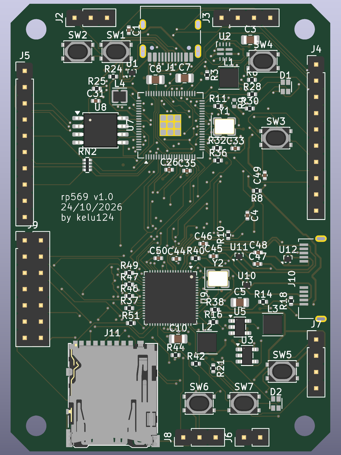
Why?
The RP2350 is a lovely chip for fast, deterministic I/O: three PIO blocks, 48 GPIOs on the QFN-80 “B” version, and enough clock to sample or generate signals at tens of MHz. What it doesn’t have is a fast way to get all that data out: its USB is full-speed, 12 Mbit/s. Ouch.
The WCH CH569 is the exact opposite: a RISC-V chip with a USB 3.0 SuperSpeed controller and a high-speed parallel interface (HSPI)… but no PIO. So why not put the two on the same board, innit? 😊
What it does
rp569 is a 50 × 70 mm, 4-layer board where the RP2350B produces data, pushes it over an 8-bit parallel bus to the CH569, and the CH569 streams it to the host over USB 3.
- RP2350B side: USB-C (USB 2.0, for firmware, debug and test control), QSPI flash, an RGB LED, two buttons, an I2C header and a 1x10 header with the ADCs and a debug UART.
- CH569 side: USB 3.0 Micro-B, a microSD slot on the eMMC/SD controller, an RGB LED, two buttons and a 2x07 header with 12 GPIOs.
- Between the two: the 8-bit HSPI bus with clock and handshake lines, a shared I2C bus and a UART. Why 8 bits and not 16? The CH569’s upper data lines share pins with the SD card, and I wanted to keep the card.
- A logic analyser for free: eight more RP2350 pins come out on a 10-pin header. PIO samples them, the samples go down the HSPI bus and out over USB 3. It’s a simple streaming logic analyser, and it gives the link a real workload.
The board is meant for automated tests, so the CH569 should never need a finger on a button: the RP2350 controls its power through a load switch, drives its reset, and can hold the boot pin low to put it in its USB bootloader. Reflashing from the host, no hands. A TI TPS2121 power mux combines the two USB inputs, so plugging both never back-feeds one into the other.
How it was made
The whole KiCad project is generated from one Python file (parts, footprints and a pin-to-net map), which writes the schematic, the placed PCB and the net classes, then runs ERC and DRC. Every part has an LCSC number so JLCPCB can assemble it, apart from the CH569W itself and the USB3 connector, which have to be consigned.
The routing was its own little adventure, from 421 open links to zero: first Freerouting (which needed a one-instruction bytecode patch before it would respect its max-passes setting!), then KiCadRoutingTools, and the last 16 links by hand. The big lesson: every real improvement came from changing the placement (picking pins by chip side, turning passives, dropping sixteen series resistors), not the router settings. Vibe-coded with my good friend Claude doing the scripting and the analysis.
Status
v1.0 is routed, with 0 unconnected nets and 0 DRC errors, and the JLCPCB production files are ready. It’s not ordered yet: the USB pairs still need re-routing as proper coupled pairs, and the silkscreen needs a clean-up. No firmware yet either, the HSPI framing and the PIO transmitter are the next big pieces. Fingers crossed =)
The build logs are on Hackaday.io, and the sources, design decisions and datasheets live on GitHub. Thanks to HydraUSB3 and phantomdrive for showing the way on the CH569 side.
