rp417 (vc)
An RP2350 babysitting a CH32H417, to push it to its limits
Why?
WCH’s CH32H417 looks like a monster on paper: a RISC-V chip with USB 3.0 SuperSpeed, a camera-style parallel capture port (DVP), a fast internal ADC, SDIO… and all of that in a QFN. On paper. Datasheets are lovely, but I wanted to know how far it really goes before building anything serious on it.
Testing that by hand is tedious: plug, flash, press reset, run, unplug, repeat. So I put a chip I know well, an RP2350, next to it and gave it the job of babysitting the CH32 so that a script on the PC can run the whole test bench. It’s the little sibling of rp569, same idea, different victim 😊
What it does
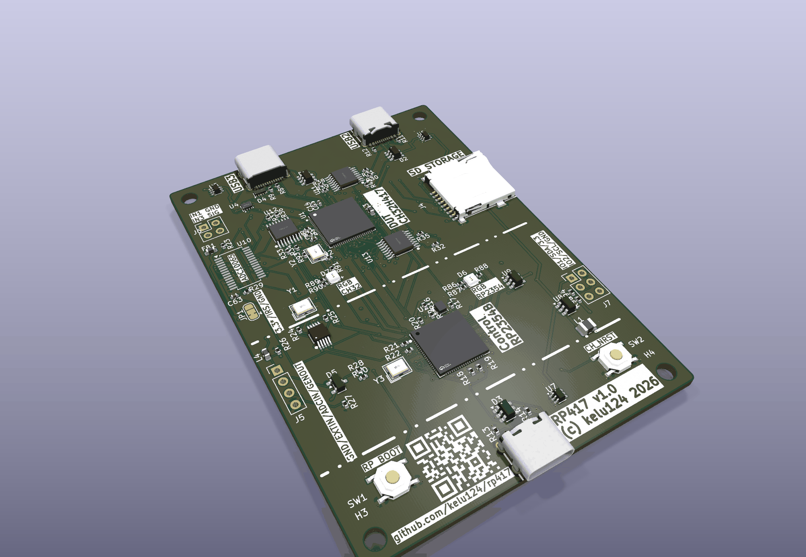
rp417 is a 6-layer, playing-card-sized board (63.5 × 88.9 mm) with an RP2354B as the supervisor and a CH32H417 as the device under test.
- The supervisor: the RP2354B is always on. It switches the CH32’s power, drives its reset, flashes it over its debug pins as a ch32fun / minichlink “funprog” programmer, and watches its supply rails with its own ADC. It talks to the CH32 over UART, I2C, QSPI and an 8-line logic bus.
- USB3 throughput: the CH32 has its own USB-C with SuperSpeed, so it can stream straight to the host. A second USB-C serves the CH32’s full-speed port (and its bootloader), a third one is for the RP2354B. Any one of the three cables powers the whole board.
- Parallel capture: a 65 MSPS 10-bit ADC (ADC10065) feeds the CH32’s DVP port… or, flip a bus switch, the RP2350’s PIO feeds it a 10-bit counter instead. A counter is the best test pattern there is: a single lost, duplicated or swapped sample shows up straight away.
- A signal source: an Si5351 clocks the ADC and the capture, and its third output goes through a small LC low-pass filter to make a roughly-sine test signal up to ~30 MHz. It’s for throughput tests rather than hi-fi, but it feeds the external ADC, the CH32’s internal ADC and its HSADC from the same source.
- And the rest: a microSD slot on the CH32’s SDIO, two RGB LEDs, two buttons and an SAO header, because why not.
The fun gotcha: the CH32’s debug pins are the same pins as its high-speed USB data lines. A small USB switch picks one or the other, and that same switch also works as a software “unplug” for the USB tests. The chip has no BOOT0 pin either, so power-cycling it from the RP2350 is also the backup way into its bootloader. No fingers on buttons, ever.
How it was made
Same recipe as rp569: the schematic is generated from Python (the netlist lives in one file), the placement too, and every design choice is written down in a numbered decision log, now at around seventy entries. One early rule shaped the board: keep the BOM minimal. Out went the DDS chip and the external power input, and in came “let the firmware switch things off in the right order” instead of isolation chips.
Freerouting did a first routed draft, then I finished the routing by hand in KiCad. The whole thing went from an empty repo to routed board with JLCPCB production files in three days. Vibe-coded with my good friend Claude, who also read the Chinese reference manuals with me (thank you, datasheet translations).
Status
v1.0 (rev A) is fully routed, and the Gerbers, BOM (with an LCSC number on every line) and placement files are ready. Not fabricated yet. The CH32 itself gets consigned to JLC, and the ADC will be hand-soldered. No firmware yet: next up is the RP2350 programmer port and the test-control interface, then actually proving gapless capture, USB3 speeds and how hot the CH32 gets at full load. Fingers crossed =)
Everything (pin map, power tree, layout, BOM, production files) is on the project site, and the sources, decision log and datasheets live on GitHub.